Research II
Presentation of
The Research Laboratory for High Voltage Electron Microscopy
The Research Laboratory for High Voltage Electron Microscopy (the HVEM Laboratory),Kyushu University, was established in December 1975 for general use by researchers and students throughout KU. Over thirty-five research programs from various fields of scientific and engineering studies are conducted annually in the laboratory. Based on the sophisticated activities through the HVEM, this laboratory has also been involved in the Nanotechnology Support Project in 2002, which was started by the Ministry of Education, Culture, Sports, Science and Technology of Japan, for the purpose of supporting research and the use of facilities. In this issue of KYUDAI NEWS, the present status and the future prospects of the laboratory are introduced, together with explanations of the necessity of electron microscopy and the advantages of the HVEM. |
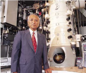
| Director |
| Chiken Kinoshita |
| Professor, Faculty of Engineering |
What is Microscopy?
It is sometimes necessary or desirable to examine the structural elements that influence the properties of materials. The capacity to perform such examinations is important firstly to ensure that the associations between the properties and structure are properly understood, and secondly to predict the properties of materials once these relationships have been established.
Both optical and electron microscopes are commonly used in microscopy. These instruments aid in investigating the microstructural features of all kinds of materials. With optical microscopy, the light microscope is used to study the microstructure; its basic elements are optical and illumination systems. For materials that are opaque to visible light (metals and many ceramics and polymers), only the surface is subject to observation, and the light microscope must be used in a reflecting mode. Contrasts in the image produced result from differences in the reflectivity of the various regions of the microstructure.
What is Electron Microscopy?
The resolving power limit of the optical microscope is approximately 0.5 μm, which is equivalent to the minimum wavelength of visible light. Consequently, some structural elements are too fine or too small to permit observation using optical microscopy. Under such circumstances the electron microscope, which is capable of much higher magnifications, may be employed.
An image of the structure under investigation is formed using beams of electrons, instead of light radiation. When accelerated across voltages larger than 200 kV, electrons can be made to have wavelengths on the order of less than 0.003 nm. The high magnifications and resolving powers of electron microscopes are consequences of the short wavelengths of electron beams. The electron beam is focused and the image formed with magnetic lenses; otherwise the geometry of the microscope components is essentially the same as with optical systems. Both transmission and reflection beam modes of operation are possible for electron microscopes.
An electron beam passes through the specimen and forms the image. It becomes possible to observe details of internal microstructural features; contrasts in the image are produced by differences in beam scattering or diffraction produced between various elements of the microstructure. Since solid materials are highly absorptive to electron beams, the specimen to be examined must be prepared in the form of a very thin foil; this ensures transmission of an appreciable fraction of the incident beam through the specimen.
Quantitative and qualitative characterizations of materials are vital for obtaining detailed structural, chemical and elemental information at the highest level of spatial resolution. Structural information can be derived from achieving the electron diffraction pattern, which reflects the 3-D atomic arrays of the materials or achieving 2-D images with atomic resolution. However, chemical information, such as the location of impurity atoms or the positions of host atoms, is more difficult to extract from plane images, and the electron microscopist often has to resort to fine-probe techniques (e.g., electron energy-loss spectroscopy or energy dispersive X-ray spectroscopy) to identify and locate chemical species.
High Voltage Electron Microscopy and Its Characteristies and Advantages
Electron microscopy using a much higher accelerating voltage than that employed in conventional electron microscopy is termed High Voltage Electron Microscopy. There is no unique transition between the two. In recent years, a new class of Medium Voltage Microscope has been developed, employing accelerating voltages in the range of 300-400 kV. High voltage in this context is therefore generally taken to refer to accelerating voltages of about 500 kV and above.
The first advantage of adopting higher operating voltages is the higher penetrating power of the electron beam. The effect is greatest for low atomic number materials, and there is a three-fold to six-fold increase in penetration between 100 and 1000kV. Since thicker samples provide more intrinsic bulk behavior, the high voltage electron microscopy is a good tool to observe not only the intrinsic structures, but also the dynamic behavior of materials. Thick samples also provide information about three-dimensional structures through stereomicroscopy.
The second advantage of high voltage electron microscopy is based on the short electron wavelength. The ultimate resolving power of electron microscopy is based on the short electron wavelength. The ultimate resolving power of electron microscope at 1000kV is improved by a factor of about three compared with that at 100 kV, and this forms the basis for high-resolution, high-voltage electron microscopy. Additionally, a relatively large pole-piece gap of objective lens is advantageous to accommodating a wide variety of specimen stages, such as the hot stage, cryogenic stage, tensile stage and others.
The final but most important consideration is that of radiation damage. In organic materials such as biological specimens, lower accelerating voltages cause more severe ionization damage. The severity of the damage decreases as the ionization cross-sections of the atoms in the sample decrease with increasing accelerating voltage. As the accelerating voltage increases, however, the increasing electron energy reaches a threshold value where electrons displace atoms from their equilibrium sites. This from of radiation damage also destroys the intrinsic structure of materials, including inorganic materials, but opens up the direct study of displacement damage processes.
The HVEM, therefore, provides many experimental advantages not only for nano-scale microstructural analysis but also for investigating radiation effects. The advantages include high electron flux, easy control of electron energy, easy alignment of crystallographic orientation, easy control of irradiation temperature and so on. However, the most important advantage of electron microscopy is that it permits direct observations of phenomena during electron irradiation.
Present Status, Activities and Future Prospects
A HVEM, JEM-1000 with the maximum accelerating voltage of 1250 kV, was installed in 1976. With the system Os overhauling and partial modifications from 1987 to 1988, a new ion-irradiation device was attached to the system and a high resolution electron microscope JEM-4000EX was also installed. Furthermore, two auxiliary electron microscopes JEM-200CX and three analytical electron microscopes, including one JEM-2000FX (1983) and two TECNAI-20 (2001 and 2003) with spectrometers for X-ray, have been introduced with a variety of attachments to the systems. A field emission electron microscope JEM-2010FEF with an in-column energy filtering system was also installed in 1995. In addition to those microscopes, equipments for specimen preparation are also available, e.g. Ar ion milling systems and focused Ga ion beam machines. The main facilities installed in the HVEM Laboratory are listed in Table 1 together with their performance, functions and characteristics.
Table 1: Transmission Electron Microscopes installed in the HVEM Laboratory and their Performance, Functions and Characteristics.| Microscope | Maximum Accelerating Voltage / Resolution | Functions | Characteristics |
| JEM-1000 | 1300 kV 0.27 nm | Electron / ion irradiation, Heating, Cooling, Elogation | HVEM-Accelerator interface facility |
| JEM-2010FEF | 200 kV 0.23 nm | Image-filter, X-ray analysis, Covergent electron diffraction, Scanning TEM, Criotransfer | Omega-type energy filter electron microscope |
| JEM-4000EX | 400 kV 0.18 nm | High resolution image | High resolution TEM |
| JEM-2000FX | 200 kV 0.28 nm | X-ray analysis, Convergent electron diffraction, Hollow cone beam | Analytical electron microscope |
| TECNAI-20 | 200 kV 0.23 nm | X-ray analysis, Scanning TEM | Digital analytical electron microscope |
Their activities and publications have been summarized in the Annual Reports of the HVEM Laboratory, No. 1-27, since the establishment of the HVEM Laboratory in 1975. More than 2300 papers have been published and about 170 doctoral theses have been approved based on the research works carried out at the HVEM Laboratory.
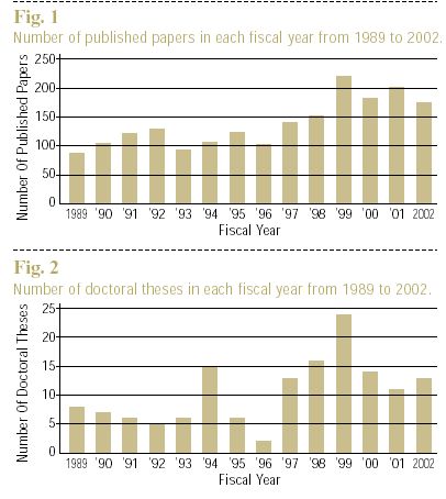
Fig. 1 and Fig.2 respectively show the numbers of published papers and approved doctoral theses in each fiscal year from 1989 to 2002. The research subjects are basically classified into the following four items:
(1) The development of sophisticated methods for preparing TEM specimens, giving instructions in the methods.
(2) In situ experiments at various temperatures (20K~1500K) under electron/ion irradiation, applied electric field and/or tensile states.
(3) The structural and compositional analysis of sub-nanometer structures, such as chemical and electronic structures.
(4) The electron microscopy for radiation sensitive materials, such as inorganic materials.
The HVEM covers main parts of nanotechnology, which is a multidisciplinary field that extends over a wide range of sciences and technologies, such as information, materials, environment and life sciences. Being aware of the importance of nanotechnology, the Ministry of Education, Culture, Sports, Science and Technology of Japan has started Nanotechnology Support Projects in 2002 for the purpose of supporting research and the use of facilities. The HVEM Laboratory was selected for support by the project on the basis of its sophisticated electron microscopy and related facilities.
Our future strategy will be to support researchers not only within KU but also outside, including universities, industries and government institutes all over the world, and to encourage collaborations among them. By pursuing this strategy, we also hope to provide a forum for university, industry and government researchers to establish a sophisticated COE of electron microscopy.