研究成果 Research Results
- TOP
- News
- Research Results
- Extraordinarily thick organic light-emitting diodes solve nagging issues
Extraordinarily thick organic light-emitting diodes solve nagging issues
2019.07.30Research ResultsMaterialsTechnology
By combining thin organic layers with thick layers of hybrid perovskite, researchers at Kyushu University in Japan have developed micrometer-thick organic light-emitting diodes that could improve the affordability and viewing angles of high-performance displays and televisions in the near future.
Organic light-emitting diodes (OLEDs) use layers of organic molecules to efficiently convert electricity into light. The molecules, though great emitters, are generally poor electrical conductors, so the name of the game has been thin—as in 100 nm, or about 1/500 the thickness of a human hair. Only by using such thin layers can electricity easily reach where emission occurs in the middle of devices.
While extremely thin layers benefit from needing only a small amount of material, the use of such thin films complicates the reliable fabrication of millions of pixels since extremely small defects can cause device failure. Furthermore, light reflecting between the front and back of the thin layers often results in interactions—called cavity effects—that slightly distort the emission color at large viewing angles.
Thus, the challenge has been to make the devices thicker while avoiding the drawbacks of organics. To do this, researchers at Kyushu University turned to an alternative class of materials called perovskites, which are defined by their distinct crystal structure.
“Although perovskites have recently attracted a huge amount of attention as light-absorbing layers in solar cells, some perovskites are actually transparent while also being highly conductive,” says Toshinori Matsushima, associate professor of the International Institute for Carbon-Neutral Energy Research at Kyushu University and lead researcher on the Nature paper announcing the new results.
“In addition, perovskites based on a blend of organic and inorganic components can be processed from low-cost starting materials using the same fabrication processes as for organics, making perovskites and organics a perfect match.”
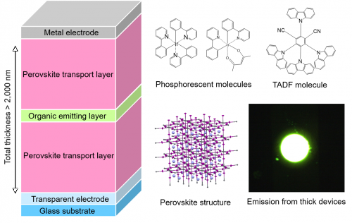
In their devices, the researchers sandwiched an emitting layer of molecules typically used in OLEDs between perovskite layers with a total thickness of 2,000 nm. The resulting devices have active layers that are 10-times thicker than typical OLEDs—though still a fraction of the width of a human hair.
The thick devices exhibited efficiencies that were similar to those in reference thin OLEDs while also having the same color from every viewing angle. On the other hand, OLEDs based on thick organic layers did not emit any light at similar operating voltages.
“These results overturn 30 years of thinking that OLEDs are limited to thin films and open new paths for low-cost, reliable, and uniform fabrication of OLED-based displays and lighting,” says Prof. Chihaya Adachi, director of Kyushu University’s Center for Organic Photonics and Electronics Research.
While researchers have also been attempting to use perovskites directly as light emitters, the lifetimes of the devices have been short so far. By keeping the emission process in the organic materials and using perovskites just for transporting electricity, the Kyushu team achieved similar lifetimes for both thick devices and reference OLEDs.
“Based on this work, perovskites will be seen in a new light as versatile, high-performance materials for supporting roles in not only OLEDs but also other organic electronic devices, such as lasers, memory devices, and sensors,” predicts Adachi.
For more information about this research, see “High performance from extraordinarily thick organic light-emitting diodes,” Toshinori Matsushima, Fatima Bencheikh, Takeshi Komino, Matthew Leyden, Atula S. D. Sandanayaka, Chuanjian Qin, and Chihaya Adachi, Nature (2019), https://doi.org/10.1038/s41586-019-1435-5
Release by William J. Potscavage Jr.

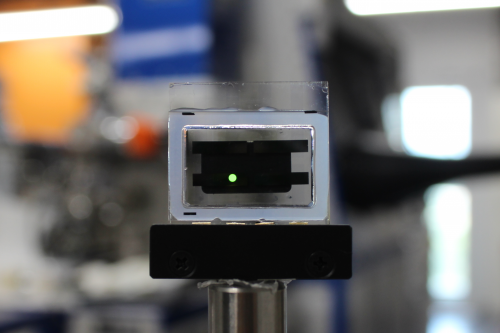
A test organic light-emitting diode (OLED) incorporating thick layers of hybrid perovskite emits green light.

The organic emitting layer was composed of molecules that show efficient phosphorescence or thermally activated delayed fluorescence (TADF). Metal halide perovskite layers, which are transparent and easily carry electricity, were placed on both sides of the organic layer. The micrometer-thick OLEDs had very high external quantum efficiencies of up to 40%. Emission spectra were independent of viewing angles for OLEDs with appropriate perovskite thickness, contributing to OLED displays with no distortion of emission color at various viewing angles.

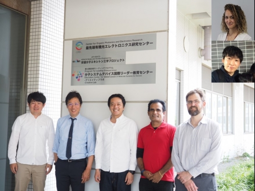
The research group at Kyushu University
Researcher comments
Over the 30 years since the first development of basic OLED architectures, researchers have thought that OLEDs are limited to thin organic films. Our idea of using thick perovskite transport layers for OLEDs overturns this traditional thinking. By further developing materials chemistry in parallel with device physics, we will pursue this new platform for fabricating next-generation devices with even higher performance and lower fabrication costs.
Journal Reference
High performance from extraordinarily thick organic light-emitting diodes, ,Nature, https://doi.org/10.1038/s41586-019-1435-5Research-related inquiries
- TOP
- News
- Research Results
- Extraordinarily thick organic light-emitting diodes solve nagging issues


