![]()


![]()
![]()
研究成果 Research Results
- TOP
- News
- Research Results
- Cheap, non-toxic material for photoactive electronics and chemistry in the spotlight
Cheap, non-toxic material for photoactive electronics and chemistry in the spotlight
Successful synthesis of perovskite visible-light-absorbing semiconductor material 2021.05.19Research ResultsPhysics & ChemistryMaterialsTechnology
H--doped BaSn0.7Y0.3O3–δ: A cheaper perovskite-based semiconductor material that is free of toxic lead and can absorb a wide range of visible light with potential photofunctional applications
Semiconductors that can exploit the omnipresent visible spectrum of light for different technological applications would serve as a boon to the material world. However, such semiconductors often do not come cheap and can often be toxic.
Now, a group of material scientists from Tokyo Institute of Technology and Kyushu University have collaborated to develop a cheaper and non-toxic narrow-gap semiconductor material with potential ‘light-based’ or photofunctional applications, according to a recent study published in Chemistry of Materials.
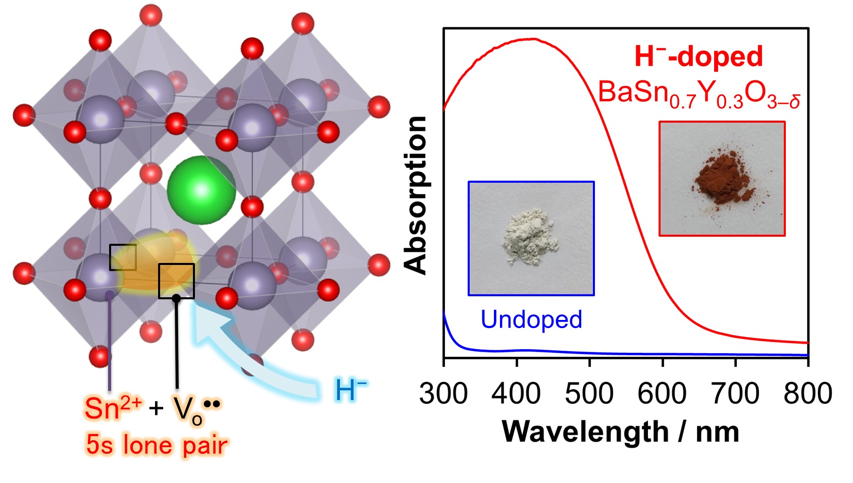
Tin-containing oxide semiconductors are cheaper than most semiconductor materials, but their photofunctional applications are constrained by a wide optical band gap. The aforementioned team of scientists, led by Dr. Kazuhiko Maeda, Associate Professor at the Department of Chemistry, Tokyo Institute of Technology, developed a perovskite-based semiconductor material that is free of toxic lead and can absorb a wide range of visible light.
The team “doped,” or intentionally introduced, hydride ions into the tin-containing semiconductor material. In doing so, they successfully reduced the band gap from 4 eV to 2 eV, due to the chemical reduction of the tin component that accompanied the hydride ion doping.
The scientists were also able to pinpoint a crucial tin reduction reaction in the semiconductor material through physicochemical measurements. This reduction leads to the generation of a “tin lone electron pair,” whose different electronic states notably contribute to the visible light absorption of the material.They also attribute this desired property to the prior introduction of oxygen defects into the material.
Highlighting the importance of the oxygen defects, Dr. Maeda, who is also a corresponding author of the study, explains, “The prior introduction of oxygen defects into BaSnO3 by Y3+ substitution for Sn4+ is also indispensable to realize a significant reduction of the band gap.”
To confirm that the developed semiconductor material is indeed photofunctional, the scientists tested the applicability of the semiconductor material in a photoelectrode. They observed that the developed material gave a clear anodic photoresponse up to the expected 600 nm.
Speaking about the impact of the study, Dr. Katsuro Hayashi, Professor of the Faculty of Engineering, Kyushu University, and the other corresponding author of the study, says, “Overall, the study has enabled a giant leap in the development of a cheaper, non-toxic, narrow optical band gap, tin-containing semiconductor material for practical applications in solar cells, photocatalysis and pigments.”
###
For more information about this research, see “Sn-based perovskite with a wide visible-light absorption band assisted by hydride doping,” Masashi Nakamura, Hiroshi Watanabe, Hirofumi Akamatsu, Kotaro Fujii, Masatomo Yashima, George Hasegawa, Miki Inada, Katsuro Hayashi, and Kazuhiko Maeda, Chemistry of Materials (2021). https://dx.doi.org/10.1021/acs.chemmater.1c00460
This release is also available in Japanese.
Research-related inquiries
Katsuro Hayashi, Professor
Department of Applied Chemistry, Faculty of Engineering
Contact information can also be found in the full release.
- TOP
- News
- Research Results
- Cheap, non-toxic material for photoactive electronics and chemistry in the spotlight